
Process Development for Advanced Nanodevices
Thermoelectric device
Thermoelectric device can directly convert heat into electricity. So, thermoelectric device have attracted in terms of energy harvesting because of diversity of energy source. Miniaturization of thermoelectric device can achieve to be mounted to various instruments, which is expected for wearable device and so on. Among some methods to fabricate micro size thermoelectric device, electrodeposition has many advantages: low-cost, rapid deposition rate, selective deposition etc. We try to take advantage of these merits of electrodeposition to fabricate micro thermoelectric device and boost these performance.
Fabrication of thermoelectric materials
In our laboratory, we use electrodeposition to fabricate materials, and focus on Bi-Te materials because they have high performance at near room temperature. Bi-Te thin films have various Seebeck coefficient (positive: p-type, negative: n-type) depending on composition of film (Fig. 1). After optimization of electrodeposition conditions, patterned electrodeposition was carried out (Fig. 2).
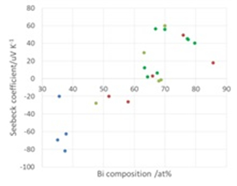
Fig. 1 Value of Seebeck coefficient
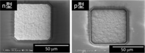
Fig. 2 SEM images of patterned electrodeposit
Fabrication of thermoelectric device
Π-structured thermoelectric device were fabricated by optimization of experimental condition. After patterned electrodeposition into 50×50 μm2 holes, 20 μm deep, and electrodeposition of upper Ni electrode (Fig. 3), performance of thermoelectric device were measured (Fig. 4). In our group, we generated 4.57 times more power (0.96 μW) by increasing upper electrode size (1.65 times larger).
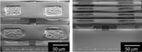
Fig. 3 SEM images of Π-structured device
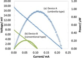
Fig. 4 Performance of device
Now, we try to further improvement by optimization of device design and studying some new materials and so on.
Wet-Chemical Process Innovation for the Fabrication Process of Bit Patterned Media
We have studied the fabrication process of ordered arrays of ferromagnetic nanodots for the use in next generation of ultra-high density magnetic recording media, such as bit-patterned media (BPM). Fabricating ordered arrays of nanodots with uniform structure using conventional methods used to form nanostructures have some difficulties. Because electrodeposition exhibits excellent features in high controllability and deposition uniformity at nanoscale, we have proposed a fabrication process of ferromagnetic nanodots by combining lithography technique and electrodeposition. As a ferromagnetic material we focused on CoPt alloys, since CoPt exhibits high coercivity without annealing treatment, it is suitable for the fundamental studies of BPM fabrication. For the fabrication of nanopore patterned substrate, we applied UV-nanoimprint lithography (UV-NIL) and electron beam lithography (EBL). Since UV-NIL utilize mold, it has advantages of high resolution and high throughput. On the other hand, EBL is a maskless lithography technique, which electron beam directly draws desired patterns in several nanometers with high resolution. Considering an application in practical media, CoPt nanodot arrays with 150 nm diameter and 300 nm pitch were fabricated on a glass disk substrate with soft magnetic underlayer (CoZrNb underlayer), which has a close layer structure with existing HDD, using UV-NIL. In addition, by optimizing the fabrication process of nanopore patterned substrate by EBL, we have succeeded to fabricate CoPt nanodot arrays with 25 nm in pitch, corresponding to 1 Tbit/in2 areal recording density.
Because our group is also interested in understanding the structure and magnetic properties of ferromagnetic alloys at a fundamental level, we also investigate the electrochemical formation of CoPt nanodot arrays inside the nanopores fabricated by EBL. For example, we analyzed the effects of applied potential on the crystal structure of nanodot arrays, and based on this detailed analyses we have succeeded to control the crystal structure to fabricated nanodot arrays with single crystal structure, which is highly desirable for the BPM application owing to its high coercivity and high crystallinity.
We are also studying the fabrication process of nanodot arrays consisting of FePt alloy, which has been proposed as a next generation materials to CoPt for the BPM application owing to the high magnetocrystalline anisotropy constant, Ku.
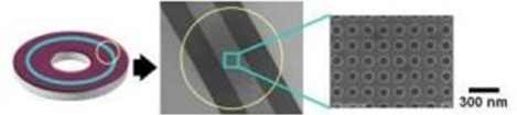
Fig.1-1 Formation of nanodot patterns on a glass disk substrate by using UV nanoimprint lithography.
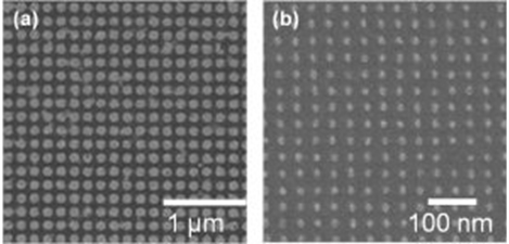
Fig.1-2 SEM images of electrochemically fabricated CoPt nanodot arrays on patterned substrates by UV-NIL(a) and EBL(b).
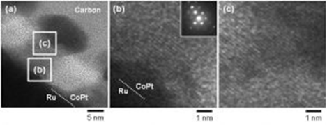
Fig.1-3 Cross-sectional TEM images of CoPt nanodot arrays having single crystal structures fabricated by precise control with applied potentials. Low magnification image (a) and high magnification images of interface between CoPt and Ru underlayr (b) and upper part of the nanodots (c).
Development of Plasmon Sensor for Surface Analysis
Estimation of phase transition and melting temperature of APTES self-assembled monolayer using surface-enhanced Raman scattering (SERS)
Surface-enhanced Raman spectroscopy (SERS) was employed to observe the kinetic phase transition of monolayer sample, 3-Aminopropyl triethoxysilane (APTES) self-assembled monolayers (SAMs). APTES is a typical organosilane agent for the preparation of amino-terminated films on silicon substrates. It is used to promote adhesion of polymer films on glass, promote protein adhesion and cell growth, and attach metal nanoparticles (NPs) to a silica substrate. The melting process of ordered structure is significant for its application because a melted (disordered) APTES monolayer could weaken the device properties and performance. However, there has been very little research on the phase transition (melting) process of an APTES SAMs.
After APTES self-assembles on a silica surface, it can maintain the solid state even under an environmental temperature above its melting point. Therefore, there must be a higher melting point and a specific melting process for an APTES SAM than for a typical standard APTES sample. However, for a sample with such an extremely thin layer structure, detailed analysis of the interior structural variation is fairly difficult to realize. To gain insight into the mechanism of the phase transition process inside an APTES monolayer and estimate the melting point, we attempted to employ anti-Stokes and Stokes surface-enhanced Raman scattering. A time-resolved measurement mode was used to monitor the variation in the Raman spectra in situ and the structural change in APTES SAMs (from ordered to disordered structure) under heating was discussed in detail, and the phase change point was calculated. We conclude that the structure of APTES SAM changed from ordered crystalline to disordered at around 118◦C.
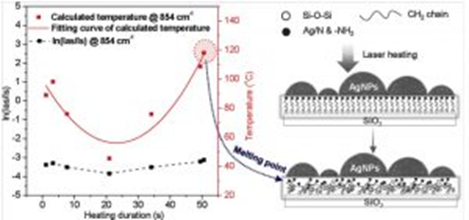
Fig.1 Calculated temperature variation during heating (left) and schematic diagram of phase change process (right) of APTES.
Analysis on Electrochemical Interfacial Process
Negative Electrode of Zn Secondary Battery
Zinc secondary battery is expected as one of the most promising candidates in terms of low cost, abundance, and its safety. Zinc primary battery has been known for over century and a lot of studies has been performed for practical secondary battery. However, since the electrode forms specifically during Zn deposition for charge and Zn stripping for discharge, this is one of the biggest issues. Especially in the discharge reaction, supersaturated zincate ion turns into ZnO (zinc oxide) to cause undesirable effects on charge/discharge reversibility. Based on past studies that show the influence of the surface morphology of Zn electrode after the charging on ZnO morphology, our group aims to acquire mechanistic understanding of the effect so as to suggest feasible method for the ZnO control. Our current study focuses on morphological difference of the Zn surface arising in the case of metal (Pb or Sn) addition in the electrolyte so that we suggest the method to control ZnO deposition behavior to achieve high reversible Zn battery construction.
Fig.1 shows SEM images of deposited Zn morphology from a) Pb and b) Sn added electrolyte. Fig.2 is ZnO morphology with 1) Pb or b) Sn. Those pictures indicate that metal additives affect not only Zn but also ZnO morphology.
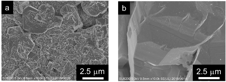
Fig.1 Deposited Zn morphology a) in Pb or b) Sn added electrolyte after charging by SEM
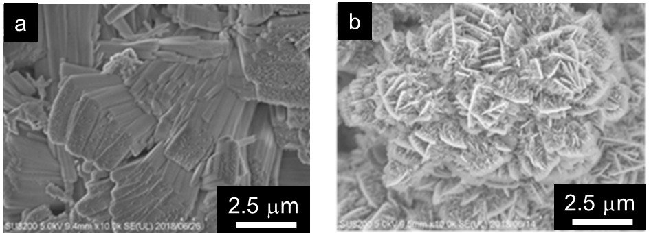
Fig.2 ZnO morphology after discharging in a) Pb added and b) Sn added electrolyte
Catalytic Electrode for Hydrogen Evolution Reaction
Hydrogen (H2) is one of the promising candidates of energy carrier in renewable energy systems. Water electrolysis is expected to be a large-scale hydrogen production process due to its simplicity and safety. Pt is still the most effective cathode material for the hydrogen evolution reaction (HER), which is, however, widely known to considerably push up the cost of the electrolysis system. That is why we have to develop new generation catalytic cathode material for the HER. When improving the HER efficiency of the electrode, we should consider H2 bubbles’ attachment on the electrode surface, because it significantly contributes to the IR loss. The fact is that this is able to be controlled by nano/micro structures of the electrode surface. We aim to propose the optimum surface structures to control bubble behaviors. For this purpose, we currently analyze the effect of surface microstructures on bubble behaviors using Ni micro-patterned electrodes, which is suitable for quantitative analysis due to its high controllability of surface structures and surface wettability.
Fig.1 represents the surface morphologies of prepared Ni micro-patterned electrodes by electrodeposition process. Fig.2 shows the evolved bubbles on the electrode surface. The larger diameter each pattern has, the more hydrogen bubbles we can see, indicating that the hydrophilicity is controlled by the structure. Currently we analyze the details of the effect of surface nano/microstructures on bubble behaviors.
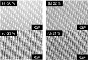
Fig.1 SEM images of prepared Nickel micro-patterned electrodes
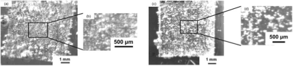
Fig.2 Bubble behaviors on the electrode surface with different Ni coverage ((a) Low Ni coverage, (b) Enlarged view of (a), (c) High Ni coverage, (d) Enlarged view of (c)
Si Purification and Electrodeposition for Photovoltaic Cell Application
Si thin films with a thickness of μm-nm order is getting attention as materials for energy products and storage device such as solar cells and electronic parts with fine structure. Our group is purifying high-purity silica, which is a raw material for solar cell grade Si, and is also preparing Si thin film for solar cells by electrodeposition.
Process Development for Si Purification
The demand for solar-grade silicon (SOG-Si) and the popularity of renewable energy have significantly increased in recent times. SOG-Si has conventionally produced via the Siemens method, which was originally developed for semiconductor-grade silicon (SEG-Si) fabrication. Disadvantage of the Siemens method include substantial energy input for purification process and the requirement of large amount of high-grade silica ore. Therefore, in order to further the development of silicon photovoltaic application, an alternative and inexpensive approach toward the generation of large quantities of SOG-Si is necessary.
Diatomaceous earth is an Earth-abundant candidate for the high-purity silica source for the resource of SOG-Si. As the main component of diatom shell is amorphous silica and it has large surface area, Diatomaceous earth easily dissolved into alkali solution. Therefore, we are investigating the production of high-purity silica from Diatomaceous earth by using aqueous chemical process. We proposed the micro size channel reactor for the extraction of light element impurities. The micro size channel reactor has advantages such as large contact area and short diffusion distance for the efficiency of liquid-liquid extraction process. And using the 2-stage extraction flow, we has been trying further efficiency of light element extraction.
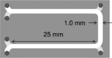
Fig.1 The schematic of 2-stage channel device
Si Photovoltaic Device
Electrodeposition has been gathering attention as the fabrication method of Si thin films because it is easy to form fine structure and can be directly formed in a cell unit at once. Therefore, our group conducts Si electrodeposition in organic solvents and ionic liquids and aim to apply the Si thin film to solar cells. In the past, we have achieved nanoscale Si electrodeposition in ionic liquids, but the unclear reaction system and inclusion of impurities have been problems. Hence, we are analyzing the mechanism of electrodeposition reaction by using electrochemical quartz-crystal microbalance, which is the method of calculating the mass change from frequency change during electrodeposition. Besides, deposition processes under the condition of light irradiation and pulsated potential signal are now studied as well. From both studies, we aim to decrease the impurities in the Si thin film. In addition, we are proceeding the formation of pn junctions for solar cells by electrodeposition.
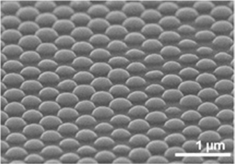
Figure 1. Si nanostructure fabricated by electrodeposition
Modeling for Electrochemical Interface Reactions
Theoretical Analysis for Reaction Mechanism of Electroless Deposition
Electrochemical reactions occurring at solid-liquid interface area between metal electrode and solution show very complex behavior, which make it difficult to understand reaction mechanisms by experimental measurements. In our team, quantum chemical calculation, which is capable to analyze the chemical system in molecular level, is applied to investigate such complicated electrochemical reaction mechanism.
We are now investigating electroless deposition as one of the major examples of solid-liquid interfacial reaction. Although this process involves many kinds of factor influencing each other complicatedly, it is possible to study the effects of these factors systematically by theoretical consideration. This section introduces some of our results, focusing on effects of metal surfaces, additives, and complexing agents.
1. Catalytic Activity of Metal Surfaces
In electroless deposition processes, reducing agents are used as electron sources. The scheme of reducing agent reaction is known to involve catalytic effects of metal surface as reaction field. If we elucidate the mechanism of the catalytic activity systematically, we should obtain helpful guidelines to suggest efficient processes. We theoretically analyzed elementary steps of such reducing agent reaction on metal surface to study the catalytic behavior of metal surfaces, focusing on characteristics of electronic state of each metal. Fig. 1 shows the reaction model of phosphinic acid on Pd surface (a), and schematic view of the mechanism of catalytic activity of metal surfaces (b). Phosphinic acid is one of the most widely used reducing agents in electroless processes. Pd and Ni were focused in this study because it is known to show strong catalytic activity on phosphinic acid reaction. Our results show that d-orbital of the metal surface plays an important role for the catalytic reaction mechanism. Similar mechanism was also seen in the reaction of another widely used reducing agent, sodium borohydride. As for the reactivity of the formaldehyde on the Cu surface, it turned out that the interaction that the intermediate shows with a water molecule and with the Cu surface is rather important than the d-band state of the metal surface.
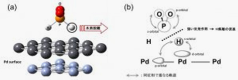
Fig. 1.1 Analysis of catalyst activity mechanism of Pd surface on phosphinic acid reaction, (a) calculation model, (b) orbital interaction between phosphinic acid and Pd surface
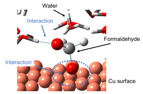
Fig.1.2 The interaction of the intermediate of formaldehyde with a water molecule and Cu surfaces
2. Additive Effects
In the electroless deposition process, trace amount of additives are added in order to control the deposition rate. If the working mechanism of this additive is elucidated at the molecular level, we can obtain important insight for efficient process design.
From this viewpoint, we theoretically analyzed working mechanism of one of the most typical additives, thiourea, in an electroless Ni deposition process using phosphinic acid as a reducing agent. Since our preliminary electrochemical measurement showed thiourea had effects mainly on phosphinic acid reaction, we theoretically investigated in detail the interaction between these two species on Ni surface. Thiourea was turned out to adsorb strongly on the surface to promote surface adsorption of phosphinic acid. Currently we are discussing more detail, combining these theoretical methods with highly sophisticated Raman spectroscopy systems.
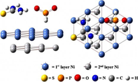
Fig. 2 Theoretical model for analyzing acting mechanism of thiourea to reaction of phosphinic acid on Ni surface
3. Complexing Agent Effects
Complexing agents in deposition bath of the electroless processes are widely known to form complexes with metal ion to stabilize the bath system under alkaline condition. But pH values of actual baths are often set to be relatively smaller, in which working mechanism of complex agents has not been clearly explained.
Our theoretical investigation of typical amino acids as widely used complexings suggests that these species are possible to form sufficiently stable complexes even under the neutral pH condition, in which water molecules play a key role. This insight should be helpful also for designs of experimental setup of electrodeposition processes and for understanding of working mechanism of chirality sensing device using self-assembled layer structure of amino acids.
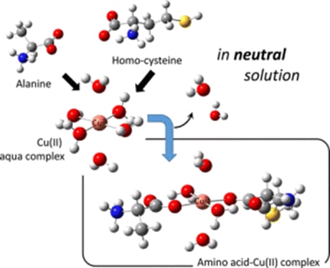
Fig. 3 Formation mechanism of amino acid copper (II) complexes